Struggling to choose between gEDA Project and DipTrace? Both products offer unique advantages, making it a tough decision.
gEDA Project is a Development solution with tags like schematic-capture, pcb-layout, simulation, eda, electronics.
It boasts features such as Schematic capture, PCB layout, Circuit simulation, Netlist generation, Bill of materials generation and pros including Free and open source, Cross-platform, Full suite of EDA tools, Active community support.
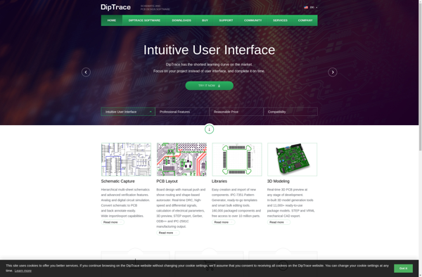
On the other hand, DipTrace is a Development product tagged with pcb, circuit-design, schematic, layout.
Its standout features include Schematic capture, PCB layout, Multilayer board design, Autorouting, 3D PCB viewing, Component libraries, Gerber file export, and it shines with pros like Affordable pricing, Easy to learn and use, Good component library, Powerful features for the price.
To help you make an informed decision, we've compiled a comprehensive comparison of these two products, delving into their features, pros, cons, pricing, and more. Get ready to explore the nuances that set them apart and determine which one is the perfect fit for your requirements.
gEDA is an open source suite of free software applications used for electronic design. It includes tools for schematic capture, PCB layout, simulation, and more. gEDA aims to provide a full workflow for designing and prototyping electronic hardware.
DipTrace is printed circuit board (PCB) design software used for schematic capture and PCB layout. It has features for multilayer boards, autorouting, component libraries, and Gerber file export.