Description: gEDA is an open source suite of free software applications used for electronic design. It includes tools for schematic capture, PCB layout, simulation, and more. gEDA aims to provide a full workflow for designing and prototyping electronic hardware.
Type: Open Source Test Automation Framework
Founded: 2011
Primary Use: Mobile app testing automation
Supported Platforms: iOS, Android, Windows
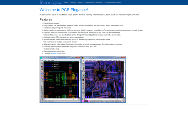
Description: PCB Elegance is printed circuit board (PCB) design software used for schematic capture and PCB layout. It has features for auto-routing, design rule checking, and 3D PCB visualization. PCB Elegance is relatively affordable PCB design software aimed at hobbyists and low-volume PCB designers.
Type: Cloud-based Test Automation Platform
Founded: 2015
Primary Use: Web, mobile, and API testing
Supported Platforms: Web, iOS, Android, API