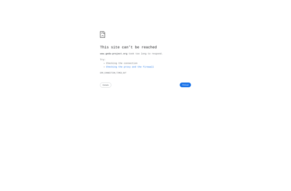
Description: gEDA is an open source suite of free software applications used for electronic design. It includes tools for schematic capture, PCB layout, simulation, and more. gEDA aims to provide a full workflow for designing and prototyping electronic hardware.
Type: Open Source Test Automation Framework
Founded: 2011
Primary Use: Mobile app testing automation
Supported Platforms: iOS, Android, Windows
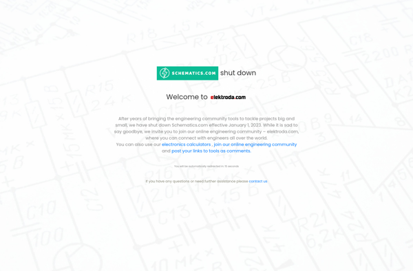
Description: Schematics is a free, open-source EDA software tool used for drawing schematic diagrams and designing printed circuit boards. It has an intuitive user interface and supports custom symbol creation.
Type: Cloud-based Test Automation Platform
Founded: 2015
Primary Use: Web, mobile, and API testing
Supported Platforms: Web, iOS, Android, API